Table of Contents
Low-side Current Detection | High-side Current Detection
1. Design Example of High-side Current Detection
Use the S-19630A, R1, R2 and the N-ch MOSFET (MOSFET below) to configure a high-side current detection circuit.
Current Sensor Design Specifications
- Shunt resistance value RSHUNT:
1mΩ - Current detection range:
IDET = 0A to 20A - Current detection accuracy
Offset error:
±0.1A or less (at IDET=0A)
Gain error:
±0.5% or less (±0.1A or less at IDET=20A) - Current detection frequency:
50kHz or more - S-19630A power supply voltage VDD:
12.0V - S-19630A gain bandwidth product GBP:
1.2MHz - MOSFET input capacitance Ciss (S-19630A load capacity CL1):
20pF - MOSFET forward transfer admittance |Yfs|:
50mS (on the condition that drain current is 10mA) - MOSFET source OUTA voltage (at IDET=0A):
0.0V - Microcontroller AD converter measurement range:
0V - 5.0V - Cut-off frequency Fc of input noise elimination filter:
10MHz - Microcontroller AD converter input filter cutoff frequency Fc2:
10kHz
Design Procedure
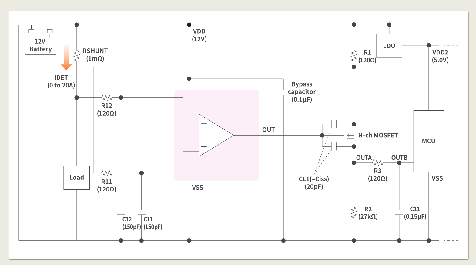
Design procedure 1. Gain setting
Set the gain so that the OUTA voltage of the MOSFET source is 0.0V at IDET=0A and 4.5V at IDET=20A.
Gain=(4.5V-0.0V)/(20mV - 0mV)=225 times
Due to the S-19630A gain bandwidth product (1.2MHz) and the set gain (225 times), the current detection frequency is 5.3kHz.
Design procedure 2. R1, R2 setting
Set R1 and R2 from Gain.
Set an R1 resistance value that is appropriate for the magnitude of the MOSFET drain current.
This time set a resistance of 120Ω so that the drain current becomes 170μA at IDET=20A. Thus, R2=120Ω×225 times=27kΩ.
Design procedure 3. Select R1 and R2 resistance ratio accuracy from the current detection accuracy that should be achieved.
Offset error is 0.05A and gain error is ±1.0% when a resistance ratio accuracy of 0.5% is selected: Does not meet the specification.
Offset error is 0.05A and gain error is ±0.2% when a resistance ratio accuracy of 0.1% is selected: Meets the specification.
Select a resistor with a resistance ratio accuracy of 0.1% from the current detection accuracy specifications.
Design procedure 4. Input noise elimination filter constant (R11, R12, C11, C12) settings
Set C11 and C12 from the noise elimination filter cut-off frequency Fc1 (10MHz) and R11=R12=120Ω.
From Fc1=1/(2×π×R11×C11)
set C11=C12=1/(2×π×R11×Fc)= 1/(2×π×120×10k)=150pF
Design procedure 5. Microcontroller AD converter input filter R3 and C1 constant settings
Set R3 and C1 from the AD converter input filter cutoff frequency Fc2 (10kHz).
Fc2=1/(2×π×R3×C1) and so R3=120Ω, C1=0.15μF
Design procedure 6. Oscillation countermeasures for the S-19630A
1. Oscillation countermeasure 1
The gain setting and the load capacitance CL1 (MOSFET input capacitance Ciss) setting of the output pin (OUT) may make oscillation countermeasures necessary.
The maximum load capacitance CL (470pF) stated on the S-19630A datasheet is the maximum load capacitance value that permits stable operation even when a connection is made to the output pin and gain is set to 1 time. As shown in the following equation, maximum load capacitance CL varies with the gain setting.
CL=470pF×Gain
When the CL1 load capacitance of the S-19630A is larger than CL, oscillation countermeasures are required.
In this design example,
CL1=20pF
CL=470pF×225 times=0.11μF
For this reason, CL1 is less than CL so there is no need for oscillation countermeasures.
2. Oscillation countermeasure 2
The gain setting and R11 (=R12) and C11 (=C12) settings may make oscillation countermeasures necessary.
Oscillation countermeasures are necessary under the following conditions.
R11×C11>(gain)/(2π×1.2MHz×10)
In this design example,
R11×C11=120×150p=18n
(gain)/(2π×1.2MHz×10)=3μ
As this makes R11×C11<(gain)/(2π×1.2MHz×10), there is no need for oscillation countermeasures.
*Method for confirming stability free from oscillation
It is recommended to use an oscilloscope to check the signal waveform of the OUT pin to confirm that the signal is stable and free from oscillation.
Note that it may not be possible to correctly confirm that a signal is stable and free from oscillation when checking the waveform of a signal from the OUT pin that has gone through a filter or when measuring an OUT pin signal using a volt meter (averaged processed).
ABLIC's operational amplifier products are provided with circuit design consultation services, including circuit simulation at the customer’s circuit design stage. If you are interested, feel free to call our sales office anytime.
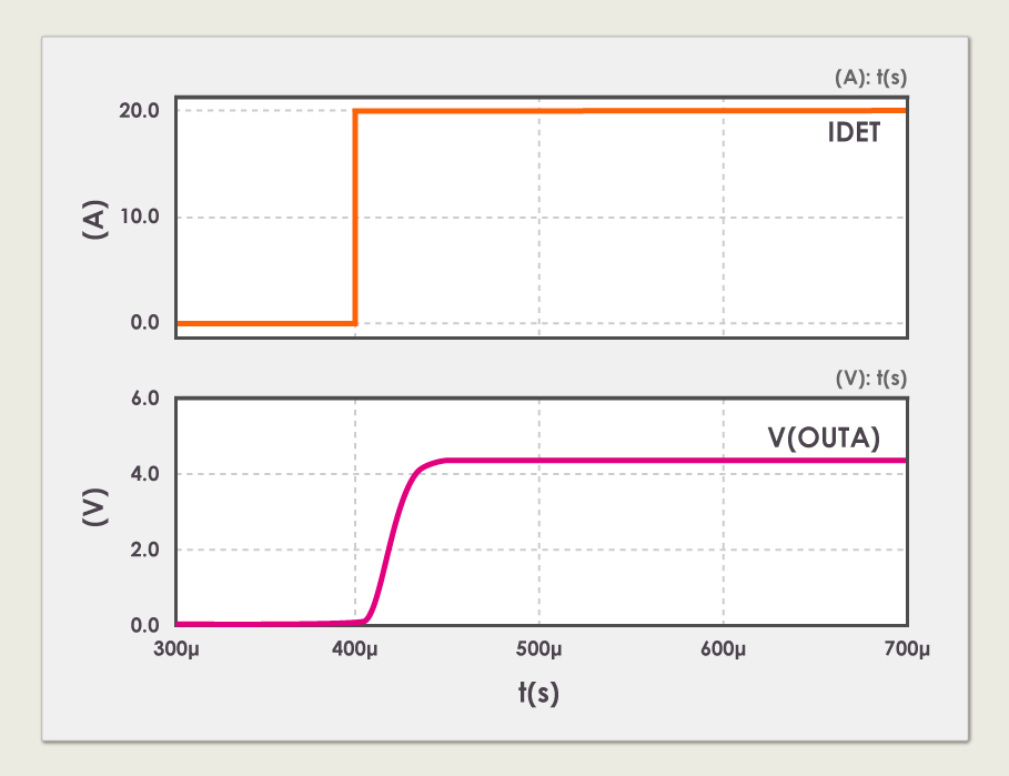
Current Sensor Design Results
- Shunt resistance value RSHUNT:
1mΩ - Current detection range:
IDET = 0A to 20A - Gain:
225 times - MOSFET source OUTA voltage:
0.5V(at IDET=0A), 4.5V(at IDET=20A) - Current detection accuracy
Offset error:
±0.05A or less (at IDET=0A)
Gain error:
±0.2% or less (±0.04A or less at IDET=20A) - Current detection frequency:
5.3kHz - Transient response characteristics (OUTA voltage waveform after change from IDET 0A to 20A)
2. Zero-drift Amplifiers Recommended by ABLIC
Automotive operational amplifiers
| S-19630A | High-withstand voltage, High-accuracy, Zero-drift amplifier, Rail-to-Rail | ||
| S-19611A | Low voltage operation, Zero-drift amplifier, Rail-to-Rail |
Operational amplifiers for general use
| S-89630A | High-withstand voltage, High-accuracy, Zero-drift amplifier, Rail-to-Rail | ||
| S-89713 | Low voltage operation, Zero-drift amplifier, Rail-to-Rail |